
ANZ ELECTRIC / SMT PROCESS ENGINEERING
SMT Stencil Design and Solder Paste Printing: A Practical Guide
Solder paste printing sits before placement and reflow, but defects introduced here can survive every downstream stage. Stencil design is the meeting point of pad geometry, paste behavior, board support and production capability.
This guide describes which variables an engineer should review with a PCB assembler. It is a decision framework rather than a universal stencil dimension table; values need to be confirmed against package guidance and the actual production process.
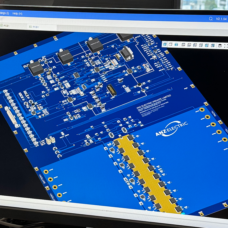 TECHNICAL WORKFLOW / 04
Why Stencil Design Matters Before Placement
An SMT stencil meters paste onto surface-mount pads. The volume and consistency of each deposit affect wetting, solder-joint formation and potential bridging or insufficient solder. ANZ's SMT assembly service describes paste printing as a controlled first step; this guide examines the engineering decisions behind it.
Start With the Land Pattern and Package Data
Review the PCB footprint, component manufacturer recommendations, solder mask definition, pad spacing, thermal pad layout and board finish. A nominal aperture should not be copied blindly from a CAD pad if the component or process calls for modification. Verify the stencil opening against the approved paste system and final land pattern.
Stencil Thickness, Aperture Geometry and Release
A thick foil may provide more paste volume but can make paste release difficult through small openings. A thin foil may favor fine features while providing too little volume for larger terminations. Aperture wall finish, geometry and print conditions also affect transfer. The industry IPC-7525 stencil design guideline describes area and aspect ratio concepts, while recognizing that a single rule cannot cover every process.
| Variable | Engineering question | Potential outcome if uncontrolled |
|---|---|---|
| Foil thickness | Does one foil serve both fine-pitch and larger pads? | Insufficient or excessive deposit |
| Aperture reduction | Does the design need controlled paste volume? | Bridging or solder starvation |
| Thermal pad pattern | Are divided apertures appropriate for the package? | Voids or float risk |
| Alignment | Do board fiducials and support hold registration? | Offset prints |
| Cleaning frequency | Can residues alter release between prints? | Print variation |
Board Support, Fiducials and Print Setup
Board flatness, stencil tension, tooling and squeegee conditions can change how much paste reaches each pad. For double-sided boards or complex panel geometries, review how the board is supported without contacting existing components. Position recognition should be stable before a production run is released.
Solder Paste Condition and Environmental Control
Paste storage, thawing, working life and mixing instructions depend on the actual supplier specification. Record material lot and opening details when they matter to the approved process. Do not invent a single temperature or time value for every solder paste formulation.
How SPI Fits the Print-Control Loop
Solder Paste Inspection (SPI) can highlight insufficient volume, excess paste, offsets or other measurable variation before placement. It should inform corrective action, not act as a substitute for good stencil and fixture design. The PCB assembly process explains where SPI fits in the overall production route.
Typical Printing Defects and Review Actions
Bridging: assess aperture, alignment and paste deposition before attributing the failure to placement. Insufficient solder: review aperture release, foil thickness, contamination and print condition. Inconsistent deposits: check board support, stencil condition, tooling and process stability. Fine-pitch behavior: review geometry and supplier package data rather than assuming generic parameters.
Stencil Design Review Checklist for an RFQ
Send the final PCB data, BOM with package identifiers, centroid, solder-mask and surface-finish information, critical package notes, planned quantity and known printing problems. Ask the assembler to identify any apertures, carrier features or process assumptions needing approval.
Related Manufacturing Decisions
- SMT assembly services — production route.
- DFM validation — footprint and spacing review.
- PCB assembly process — SPI and release gates.
For a project-specific review, send your production package to ANZ Electric.
Frequently Asked Questions
Is stencil thickness selected from the smallest SMT component alone?
No. The full board, aperture-release limits, larger termination paste demand and process constraints must be considered together.
Does SPI replace a stencil design review?
No. SPI measures print outcomes; stencil and print-process design determine whether deposits can be produced consistently.
Can the same stencil design work for every solder paste?
Not necessarily. Paste properties, aperture finish, printer settings and component requirements can change the optimal design.
What should be sent for stencil review?
Current Gerber/ODB++, component packages, BOM, centroid, solder-mask information, production quantity and any critical print observations.